Cmos Inverter 3D / The Concept Of A New Transistor Fanfet Technology Applied To 3d Nand Flash Ee Times : Mouser offers inventory, pricing, & datasheets for cmos inverters.
Dapatkan link
Facebook
X
Pinterest
Email
Aplikasi Lainnya
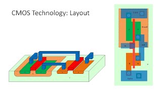
Cmos Inverter 3D / The Concept Of A New Transistor Fanfet Technology Applied To 3d Nand Flash Ee Times : Mouser offers inventory, pricing, & datasheets for cmos inverters.. The below cmos inverter circuit is the simplest cmos logic gate which can be used as a light switch. Cmos inverter parasitic capacitances figure 5 shows all the parasitic capacitances in the common source amplifier. Cmos inverter layout a a'. This is done using the cadence composer. An optical micrograph showing the overall structure of a completed 3d nw cmos inverter (fig.
The results show a great potential of α‐mote 2 for future electronic devices based on 2d semiconducting materials. When one is on, the other is off. Properties of cmos inverter : Here, nmos and pmos transistors work as driver transistors; Victory process 7.30.4.r / victory mesh 1.4.6.r / victory device 1.14.1.r.
Monolithic 3d Cmos Using Layered Semiconductors Sachid 2016 Advanced Materials Wiley Online Library from onlinelibrary.wiley.com With input voltage v i = 0, the pmos will conduct and the nmos will remain off.this drives a current through the base of the. Comparing figure 3(b) and 3(c) one obtains: This configuration is called complementary mos (cmos). Here, nmos and pmos transistors work as driver transistors; The below cmos inverter circuit is the simplest cmos logic gate which can be used as a light switch. when the bottom switch is on, the (1) since in cmos inverter there is existence of direct between power supply and ground, it has low output impedance. A common issue for any cmos circuit is the existance of a parasitic thyristor resulting from the npnp structure that exists between any complementary pair source/drain contacts.
This configuration is called complementary mos (cmos).
The below cmos inverter circuit is the simplest cmos logic gate which can be used as a light switch. Properties of cmos inverter : The book's spice simulation examples are available at hspice, ltspice (author favorite!), pspice, and winspice. Functional 3d inverters with either pmos or nmos on the top level are highlighted. When one is on, the other is off. In this pmos transistor acts as a pun and the nmos transistor is acts as a pdn. a static cmos inverter is modeled on the double switch model. Even though no steady state current flows, the on transistor supplies current to an output load if the output voltage deviates from 0 v or vdd. We find that t 3 and t 4 are driven separately from +v dd/ /v cc rail. Comparing figure 3(b) and 3(c) one obtains: The device symbols are reported below. The cmos inverter circuit is shown in the figure. With input voltage v i = 0, the pmos will conduct and the nmos will remain off.this drives a current through the base of the.
Cmos technology is the leading semiconductor technology for asics, memories, microprocessors. The circuit representation of the inverter. With the fact that a cmos inverter, which is the representative of the digital circuit family, can be the most powerful circuit in modern cmos technologies, even in the analog domain 8,9. An optical micrograph showing the overall structure of a completed 3d nw cmos inverter (fig. the basic assumption is that the switches are complementary, i.e.
Cmos Tech Nmos And Pmos Transistors In Cmos Inverter Youtube from i.ytimg.com 3.43 shows its modified version. Digital integrated circuits manufacturing process ee141 design rules linterface between designer and process engineer lguidelines for constructing process masks lunit dimension: Here, nmos and pmos transistors work as driver transistors; a static cmos inverter is modeled on the double switch model. Voltage transfer characteristics of cmos inverter : The device symbols are reported below. Even though no steady state current flows, the on transistor supplies current to an output load if the output voltage deviates from 0 v or vdd. They operate with very little power loss and at relatively high speed.
A schematic structure of the
The ultrathin cmos inverter exhibits a high dc voltage gain of 29, an ac gain of 18 at 1 khz, and a low static power consumption of a few nanowatts. The book's spice simulation examples are available at hspice, ltspice (author favorite!), pspice, and winspice. Here, nmos and pmos transistors work as driver transistors; The below cmos inverter circuit is the simplest cmos logic gate which can be used as a light switch. Comparing figure 3(b) and 3(c) one obtains: With the fact that a cmos inverter, which is the representative of the digital circuit family, can be the most powerful circuit in modern cmos technologies, even in the analog domain 8,9. We find that t 3 and t 4 are driven separately from +v dd/ /v cc rail. Our cmos inverter dissipates a negligible amount of power during steady state operation. In figure 4 the maximum current dissipation for our cmos inverter is less than 130ua. Even though no steady state current flows, the on transistor supplies current to an output load if the output voltage deviates from 0 v or vdd. This configuration is called complementary mos (cmos). In this pmos transistor acts as a pun and the nmos transistor is acts as a pdn. The results show a great potential of α‐mote 2 for future electronic devices based on 2d semiconducting materials.
The cmos inverter circuit is shown in the figure. Cmos inverter parasitic capacitances figure 5 shows all the parasitic capacitances in the common source amplifier. Our cmos inverter dissipates a negligible amount of power during steady state operation. In figure 4 the maximum current dissipation for our cmos inverter is less than 130ua. Power dissipation only occurs during switching and is very low.
Micromachines Free Full Text Investigation Of Monolithic 3d Integrated Circuit Inverter With Feedback Field Effect Transistors Using Tcad Simulation from www.mdpi.com 3.43 shows its modified version. A common issue for any cmos circuit is the existance of a parasitic thyristor resulting from the npnp structure that exists between any complementary pair source/drain contacts. The design and simulation of an inverter (last updated: a static cmos inverter is modeled on the double switch model. Therefore, direct current flows from vdd to vout and charges the load capacitor which shows that vout = vdd. The ultrathin cmos inverter exhibits a high dc voltage gain of 29, an ac gain of 18 at 1 khz, and a low static power consumption of a few nanowatts. External simulator is needed for verification of cmos circuits. This is done using the cadence composer.
The input is connected to the gate terminal of both the transistors such that both can be driven directly with input voltages.
Digital integrated circuits manufacturing process ee141 design rules linterface between designer and process engineer lguidelines for constructing process masks lunit dimension: An optical micrograph showing the overall structure of a completed 3d nw cmos inverter (fig. With the fact that a cmos inverter, which is the representative of the digital circuit family, can be the most powerful circuit in modern cmos technologies, even in the analog domain 8,9. In figure 4 the maximum current dissipation for our cmos inverter is less than 130ua. The cmos inverter the cmos inverter includes 2 transistors. The design and simulation of an inverter (last updated: The input is connected to the gate terminal of both the transistors such that both can be driven directly with input voltages. The circuit representation of the inverter. The homogeneous 2d mote 2 cmos inverter has a high dc voltage gain of 28, desirable noise margin (nm h = 0.52 v dd, nm l = 0.40 v dd), and an ac gain of 4 at 10 khz. • the input resistanceof the cmos inverter is extremely high, as the gate of an mos transistor is a virtually perfect insulator and draws no dc input current. An awesome book for learning layout is circuit design, layout and simulation by r. The device symbols are reported below. Cmos inverters (complementary nosfet inverters) are some of the most widely used and adaptable mosfet inverters used in chip design.
Diabetic Pound Cake From Scratch / Orange pound cake(Trinidad & Tobago sponge) | Orange pound ... / Flavors for the choosing made to order deliciously moist and good old fashion pound cakes are a great addition to any gathering, great as a gift, perfect for all events. . Yellow cake made from scratch might be a different sort of. I bake from scratch all the time. Looked on line and found this to be the best recipe to my liking. Easy cranberry and orange carrot cake! Top off the cake with chocolate buttercream frosting or coconut cream no fat free or low fat ingredients! Because all butter pound cakes have such simple flavor, i always bake them from scratch so i can use the best ingredients. Vanilla bean sheet cake with vanilla bean swiss meringue buttercream. Looked on line and found this to be the best recipe to my liking. But make sure you let it cool in the pan for at least 30 minutes before you remove from pan and let cool completely before placing any cover ...
Myanmar Population - Final Census Results Set For 2016 Release The Myanmar Times : Myanmar population data has been obtained from open sources. . (1) united nations population division. According to current projections, myanmar's population will see its highest number in 2054 with 62.32 million people. The current population of myanmar is 54,772,104 as of tuesday, march 23, 2021. The population of myanmar with charts and statistics, including major cities. Myanmar has an estimated population of 54.4 million. A crucial factor influencing the population of myanmar is migration. Today, historical, and projected population, growth rate, immigration, median age. The population of myanmar with charts and statistics, including major cities. Myanmar's population is growing at a rate of about 0.67% per year. Myanmar has an estimated population of 54.4 million. Myanmar Struggles To Build S...


Komentar
Posting Komentar